**Ultra-Low Jitter Clock Fanout Buffer: A Deep Dive into the ADCLK846BCPZ**
In the realm of high-speed data acquisition, telecommunications, and advanced instrumentation, the integrity of the clock signal is paramount. It is the heartbeat of the system, and any degradation in its quality directly impacts performance. This is where clock fanout buffers, specifically those engineered for ultra-low jitter, become critical components. The **ADCLK846BCPZ from Analog Devices** stands as a premier example of such a device, designed to distribute pristine clock signals across multiple destinations with minimal added phase noise.
The primary function of any fanout buffer is to take a single input clock and generate multiple identical output copies. However, a standard buffer can introduce significant jitter and phase noise, corrupting the signal it is meant to preserve. The **ADCLK846BCPZ** distinguishes itself by addressing this very challenge head-on. It is a **1:6 LVCMOS/LVTTL fanout buffer** renowned for its exceptional jitter performance. With an **additive phase jitter of a remarkably low 26 fs** (typical, 12 kHz to 20 MHz integration range), it ensures that the timing accuracy of the original clock is maintained with virtually no degradation. This performance is crucial for applications like **JESD204B/C serial link interfaces**, high-speed ADCs/DACs, and wireless infrastructure, where picosecond or even femtosecond timing errors can lead to increased bit error rates (BER) and reduced system resolution.

Several key architectural features enable this world-class performance. The device operates over a wide supply range of 2.375 V to 3.465 V, making it compatible with various system voltages. Its inputs can accept **frequencies up to 1.6 GHz (LVCMOS) and 2.0 GHz (LVPECL)**, offering flexibility in sourcing the reference clock. Each of the six outputs can be individually powered down, providing system designers with valuable power management capabilities to minimize consumption in standby or low-power modes.
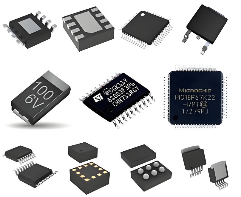
Furthermore, the ADCLK846BCPZ incorporates internal termination and is built on a proprietary Silicon-Germanium (SiGe) BiCMOS process. This advanced semiconductor technology is a significant contributor to its high-speed operation and low noise characteristics, allowing it to achieve a fast rise/fall time while maintaining excellent signal integrity. Housed in a compact 5mm x 5mm, 32-lead LFCSP package, it offers high performance in a minimal footprint, which is essential for space-constrained PCB designs.
In practice, integrating the ADCLK846BCPZ simplifies clock tree design. It eliminates the need for multiple discrete buffers and their associated matching challenges, reducing both board space and potential impedance mismatches that can generate jitter. Its robust design ensures high reliability and consistent performance across temperature and supply voltage variations.
**ICGOO**DFIND: The ADCLK846BCPZ is an **ultra-high-performance clock fanout buffer** that sets the benchmark for low jitter distribution. Its **exceptional 26 fs additive jitter**, flexible power management, and wide frequency range make it an indispensable component for designers pushing the limits of speed and accuracy in modern electronic systems.
**Keywords:** Ultra-Low Jitter, Clock Fanout Buffer, Additive Phase Noise, JESD204B, High-Speed Data Conversion
